
How Does an Electronic PCB Board Function?
Electronic PCB Board Function
An electronic pcb board functions by providing a series of conductive pathways through which electrical signals travel. These pathways, which are made of copper, are etched onto the surface of the circuit board and help ensure that signals reach their intended destinations without interference or distortion. The PCB can also include other materials, such as plastic or fiberglass, depending on the specific application.
Before the advent of the PCB, electronic components were connected to each other with wires that tangled easily and caused other problems. These issues, along with the time and labor involved in wiring multiple components together, resulted in slow development times, expensive production, and low reliability. The development of the circuit board has helped reduce costs and speed up production time, while increasing the reliability of electronics products.
The first step in the electronic pcb board design process is called capture, in which graphical symbols are used to represent components and their connections on a computer screen. The captured schematic is then simulated using SPICE to check the circuit’s integrity and determine how well it will perform under real-world workload conditions. This helps to identify errors and bugs in the design before it is physically manufactured, which saves both time and money.
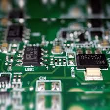
How Does an Electronic PCB Board Function?
Next comes the layout stage, in which the components are arranged on the board to meet its mechanical requirements. The layout is completed using ECAD tools, which use the information provided by the schematic to create a map of the circuit board’s traces and connections. The tools may have built-in rules that prevent a net’s traces from touching each other or from crossing each other, as well as set the width and placement of vias to avoid signal interference.
Once the component layout is complete, the assembler places the components on the traces and solder them in place. This can be done manually for small-scale production and prototyping, or by automated machines known as pick-and-place machines. The assembler can use either through-hole technology, in which the component leads are inserted through holes in the PCB and then soldered to copper pads on the opposite side, or surface mount technology, in which the component leads are attached directly to the traces using solder paste and a reflow process.
The final step in the assembly process is inspection, in which the assembler checks the quality of the circuit board. The assembler looks for signs of short-circuiting or other defects, such as breaks in the copper traces. If any of these are found, the assembler must discard the defective boards and start again. The assembler also looks for polarity errors, such as when the positive and negative leads are not connected properly to each other. This can be a serious problem in high-speed circuits, as it can lead to overheating and possible failure. The assembler can also look for signs of physical damage to the circuit board, such as scratches and cracks.