
What Is Sequential Lamination in Flex Circuits?
Sequential Lamination in Flex Circuits
When designing a PCB, you need to consider the materials used. The substrate material can make a difference between a flexible or rigid circuit board. The coverlay and adhesive materials can also play a role in how the final product will perform. The flex PCB layout should be designed according to the desired functionality of the final product. This includes identifying the conductive and non-conductive layers. It’s also important to collaborate with the additive manufacturing or mechanical engineer to ensure that the flex circuit will fit into the device.
In a multilayer flex circuit, each layer of copper must be separated by dielectric material. This is done by using sequential lamination. The sequence involves applying a layer of epoxy-based dielectric material to the surface of the substrate, then placing a thin layer of conductive material on top of it. This is then bonded together with heat and pressure. This process is repeated for each new layer. During the sequencing, each layer must be carefully inspected to ensure that it’s properly bonded and plated.
The process of assembling a flex circuit can be complicated, but it’s necessary for the production of a high-quality finished product. It requires the use of a variety of materials to create the circuit, including the copper foil. The foil may be either rolled or electroplated, with both having different properties. The copper foil should be carefully inspected and cleaned to remove any contaminants before it’s placed on the substrate. This will help prevent shorts and reduce the chance of a failure during assembly.
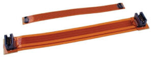
What Is Sequential Lamination in Flex Circuits?
During the manufacturing of HDI (High-Density Interconnect) printed circuit boards, the sequential lamination process is essential for routing fine-pitch, densely packed designs. This is because the process allows for more layers and more avenues to connect components within a PCB.
Sequential lamination can be a difficult process to master, but there are certain design and manufacturing guidelines that can help mitigate its challenges. These include reducing layer count, minimizing copper weights, choosing high glass transition temperature (Tg) materials, and using thin resin materials next to surface copper layers. In addition, back-drilling through-vias can reduce the need for buried or blind vias.
The sequential lamination process is the key to producing high-quality flex circuits that are robust and reliable. This process can be costly, but it offers a number of advantages that other methods cannot match. The ability to avoid misalignment and voids is one of the biggest advantages, as it can significantly reduce production costs. Moreover, it can ensure that the layers are positioned accurately and that connections are made without interference. This can be very crucial in applications that require a high level of performance. For this reason, it’s a popular choice for high-density circuits.