
How HDI Technology Enables Smaller Electronic Devices
HDI Technology Enables
As digital technology continues to advance, electronic devices are becoming smaller in size. This is due to the development of new technologies that make it possible for manufacturers to pack more components into a compact space. One such technology is High Density Interconnect (HDI) Printed Circuit Boards. These PCBs have a higher number of circuitry connections in a smaller area, which helps to reduce the size of electronic products without sacrificing performance or functionality.
The use of HDI technology in PCBs enables manufacturers to create more complex designs with shorter signal paths and less power consumption. It also allows for the integration of more components into a single board, which is beneficial in terms of cost-efficiency and weight reduction. This is particularly important for mobile / cellular phones and other portable electronics that need to be lightweight in order to comfortably fit into the user’s hand.
An hdi circuit boards is a multilayer PCB that uses a unique layering technique to achieve high-density routing. It is comprised of multiple sequential laminations that are bonded together using various methods, including thermal and chemical curing processes. These layers are then filled with either blind or buried vias to form the interconnects on the PCB. The number of sequential laminations required depends on the design specifications, as well as the type of via structure desired.
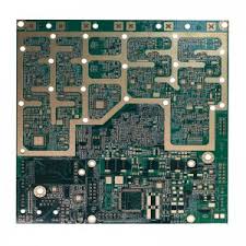
How HDI Technology Enables Smaller Electronic Devices
In addition to increasing the number of layers, HDI technology also makes it possible to increase routing density by utilizing microvias in the construction of the PCB. These vias are usually less than 150um or 6mils in diameter and are made through a combination of laser drilling and photoimaging techniques, followed by metallization and lamination to produce the PCB.
The benefits of HDI technology extend to a variety of applications, such as mobile / cellular phones, touch-screen devices, laptop computers and digital cameras. The ability to pack more components into a smaller space makes it easier to develop and manufacture these types of products. It also enables more features to be built into the device, which enhances its functionality and improves user experience.
Another benefit of HDI technology is the improved electrical performance that results from a shorter distance between components and reduced signal loss. This is because it is possible to pack more transistors onto the same board, which leads to faster signals and a significant reduction in signal crossing delays and power consumption.
As with any other PCB, it is essential that the components used on an HDI circuit board be carefully selected to ensure optimal performance. This is especially true for high-speed digital circuits, where careful layout and design is needed to maintain signal integrity, power distribution, and thermal management. A reputable PCB supplier will be able to provide expert guidance and support throughout the design process, as well as offer a quick turnaround on orders to meet tight deadlines. The right partner will be able to provide a quality product at an affordable price, which is critical for ensuring cost-effectiveness in the long term.